

Goa building a semiconductor ecosystem through academia, innovation and startups
As India accelerates its ambition to become a global semiconductor hub, Goa is steadily positioning itself within the country’s growing chip design and electronics ecosystem. Through specialised semiconductor and Very Large Scale Integrated (VLSI) laboratories, curriculum integration under the Government of India’s Chips to Startup (C2S) Programme and increasing industry-academia collaboration, the State is preparing a future-ready workforce aligned with India’s rapidly expanding electronics and semiconductor sector.
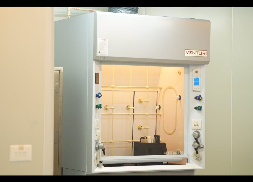
Four leading institutions including National Institute of Technology Goa, BITS Pilani K K Birla Goa Campus, Indian Institute of Technology Goa and Goa College of Engineering have strengthened semiconductor education, research and design capabilities through advanced laboratories, specialised programmes and access to industry-standard Electronic Design Automation (EDA) tools. Under the broader C2S ecosystem, these institutions have been provisioned with leading semiconductor design platforms including Synopsys, Cadence, Siemens EDA, Ansys, Keysight, Silvaco, Cadre and Compcarta, enabling students and researchers to gain hands-on experience in chip design, verification and embedded systems development.
Hon’ble Minister for Information Technology, Electronics and Communications, Shri Rohan Khaunte, has consistently highlighted the importance of creating innovation-driven ecosystems, strengthening industry-academia collaboration and preparing Goa’s youth for opportunities in emerging technologies. The State’s growing semiconductor ecosystem aligns with this broader vision of positioning Goa as a knowledge-driven and technology-enabled destination for future industries.
The semiconductor ecosystem in Goa is also creating opportunities for startups and innovation-led enterprises. Through access to advanced design tools, prototyping facilities and technical expertise, startups working in electronics, IoT, robotics, automation, medical electronics, defence technologies and AI-enabled hardware can accelerate product development and innovation. The ChipIN Centre established under the C2S Programme further supports academia, startups and MSMEs through access to semiconductor design tools, fabrication support, testing infrastructure and cloud-based chip design environments. The presence of semiconductor-focused laboratories within academic institutions is helping bridge the gap between classroom learning and industry requirements.
Beyond semiconductor education, Goa’s innovation ecosystem is also being strengthened through the BITS BioCyTiH Foundation at BITS Pilani K K Birla Goa Campus, a Technology Innovation Hub established under the National Mission on Interdisciplinary Cyber-Physical Systems with support from the Department of Science and Technology, Government of India. The Foundation enables innovators, researchers, startups and MSMEs to translate ideas into market-ready products through access to advanced research facilities, funding, mentorship and incubation support. Since its inception, it has supported 62 startups, resulting in more than 30 patents, with several technologies already licensed to industry. Its state-of-the-art Device Laboratory also provides access to advanced semiconductor, sensor and deep-tech fabrication capabilities, supporting innovation across electronics, healthcare, agriculture, water technologies and advanced manufacturing.
Nitesh B. Guinde, Professor, Goa College of Engineering, stated, “Academic institutions have a vital role in strengthening Goa’s semiconductor ecosystem by developing skilled talent, promoting research, and fostering innovation. At Goa College of Engineering, through our B.E. in Electronics Engineering (VLSI Design & Technology) programme and our participation in the Government of India’s Chips to Startup (C2S) initiative, we are providing students with exposure to semiconductor design, VLSI systems, FPGA development, and industry-standard design tools. By strengthening industry-academia collaboration and encouraging entrepreneurship, we can create opportunities for startups, attract investment, and position Goa as an emerging hub for semiconductor design and innovation.”
The growing interest in semiconductor education is also reflected in student enrolment at Goa College of Engineering’s B.E. in Electronics Engineering (VLSI Design & Technology) programme. The programme currently has around 254 students enrolled across all four years, with a new batch of admissions scheduled to commence this month. Alongside specialised academic programmes, research-led innovation hubs and advanced prototyping facilities across Goa’s premier institutions are enabling students, researchers and entrepreneurs to collaborate on industry-focused solutions, further strengthening the State’s semiconductor and deep-tech ecosystem.
These efforts are part of the broader national momentum created through initiatives such as Digital India, Skill India, Make in India and the India Semiconductor Mission. Complementing these initiatives, the Department of Information Technology, Electronics & Communications is facilitating the development of the Electronic Manufacturing Cluster (EMC) in Goa, while institutions such as BITS Pilani, IIT Goa, NIT Goa and Goa College of Engineering continue to strengthen semiconductor research, talent development and startup-led innovation. Together, these efforts are creating a strong link between education, research, entrepreneurship and manufacturing-led employment opportunities.
With continued investments in semiconductor education, research infrastructure, startup support and advanced manufacturing, Goa is building a future-ready talent pool equipped to meet the evolving needs of the electronics and semiconductor industry. These efforts are expected to generate high-value employment, encourage innovation and strengthen the State’s role in India’s expanding technology ecosystem.





 Loading ...